+86 134 0021 8776
+86 134 0021 8776
May. 08, 2023
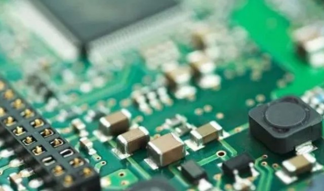
HDI (High Density Interconnect board) is a compact circuit board designed for small volume users. Compared with ordinary pcb, the most significant feature of HDI is high wiring density. The differences between the two are mainly reflected in the following four aspects.
1.HDI is smaller and lighter
The HDI board is composed of traditional double panels as core panels, which are continuously laminated. This type of circuit board is also called Build-up Multilayer (BUM). Compared with the traditional circuit board, HDI circuit board has the advantages of "light, thin, short, small".
The electrical interconnection between the boards of HDI is realized through the conductive through hole, buried hole and blind hole connection. Its structure is different from that of ordinary multilayer circuit board, and a large number of micro-buried blind holes are used in HDI board. HDI's are drilled directly with lasers, while standard PCBS are usually drilled mechanically, so the number of layers and aspect ratio tend to be reduced.
2.HDI motherboard production process
HDI board density is mainly reflected in the hole, line, pad density, layer thickness of these points.
● Micro pilot hole. The HDI plate contains blind holes and other micro-pilot hole design, which is mainly reflected in the microhole pore-forming technology with aperture less than 150um and the high requirements of cost, production efficiency and hole position precision control. In traditional multilayer circuit boards, there are only through holes without tiny buried blind holes.
● Fine line width and line distance. Its main performance in wire defects and wire surface roughness requirements are more and more strict. Generally, the line width and line distance do not exceed 76.2um.
● High pad density. The density of welded contacts is greater than 50 per square centimeter.
● Thin type of medium thickness. It is mainly manifested in the trend of the thickness of the interlayer medium to 80um or below, and the requirement of thickness uniformity is more and more strict, especially for the high-density plate and packaging substrate with characteristic impedance control.

3. HDI board has better electrical performance
HDI not only enables smaller end-product designs, but also meets higher standards of electronic performance and efficiency.
The increased interconnection density of HDI allows for enhanced signal strength and improved reliability. In addition, HDI board for radio frequency interference, electromagnetic wave interference, static release, heat conduction has better improvement. HDI also adopts full digital signal process control (DSP) technology and a number of patented technologies, with a full range of load adaptability and strong short-term overload capability.
4. The HDI board has very high requirements on the buried hole plug hole
As can be seen from the above, HDI is superior to ordinary PCB in both volume and electrical performance. Every coin has two sides, the other side of HDI is as a high-end PCB manufacturing, its manufacturing threshold and process difficulty are much higher than ordinary PCB, the production should pay attention to more problems - especially the buried hole plug hole.
At present, the core pain point and difficulty of HDI manufacturing is the buried hole plug hole. If the HDI hole plug hole is not done well, there will be major quality problems, including uneven edge concave and convex, uneven medium thickness, pad pit state, etc.
● The surface of the board is not smooth, the line is not straight in the depression cause the beach phenomenon, will cause the line gap, broken line and other defects;
● The characteristic impedance will also fluctuate due to the uneven thickness of the dielectric and signal instability;
● The uneven pad makes the subsequent poor packaging quality resulting in the joint loss of components.
Next: What is the difference between the manufacturing process of thin film and thick film resistors?
Hot Products
Navigation
+86 134 0021 8776
Floor 9, Aupu building, No. 395 XinShi North Road, Shijiazhuang Hebei, China
Request a Quote
