+86 134 0021 8776
+86 134 0021 8776
Jul. 04, 2023
1. What is back drill?
Back drilling is actually a special kind of deep drilling, in the production of multi-layer boards, such as the production of 12-layer boards, we need to connect the first layer to the ninth layer, usually we drill through the hole (one drill), and then copper. In this way, the 1st floor is directly connected to the 12th floor. In fact, we only need the 1st floor to be connected to the 9th floor, and the 10th to 12th floors are like a pillar because there are no lines to connect them. This column affects the signal path and can cause signal integrity problems in communication signals. So this extra pillar (known in the industry as STUB) is drilled from the opposite side (secondary drilling). So it is called back drilling, but it is generally not so clean, because the subsequent process will electrolyze a little copper, and the drill tip itself is also sharp. Therefore, PCB manufacturers will leave a small point, and the length of the STUB left is called the B value, generally in the range of 50-150UM.
2. What are the advantages of back drilling?
1) Reduce noise interference;
2) Improve signal integrity;
3) The local plate thickness becomes smaller;
4)Reduce the use of buried blind holes and reduce the difficulty of PCB production.

3.What is the role of back drilling?
The function of back drilling is to drill out the through hole segment that does not play any connection or transmission role, to avoid the reflection, scattering, delay, etc., which causes the signal to bring "distortion". The research shows that the main factors affecting the signal integrity of the signal system are in addition to the design, plate material, transmission line, connector, chip package and other factors, and the through hole has a greater impact on the signal integrity.
5. Back drill production process?
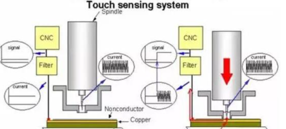
a, PCB is provided, the PCB is provided with a positioning hole, using the positioning hole for a drilling position of the PCB and a drilling hole;
b, the PCB after drilling is electroplated, and the positioning hole is dry film sealing treatment before electroplating;
c, make the outer layer graphics on the PCB after electroplating;
d. Graphic plating is carried out on the PCB after forming the outer graphic, and dry film sealing is carried out on the positioning hole before the graphic plating;
e. Use the positioning hole used by the first drill for backdrilling positioning, and use the drill knife to backdrill the electroplating hole that needs to be backdrilled;
f. After back drilling, wash the back drilling hole to remove the residual drilling cuttings in the back drilling hole.
6. What are the technical characteristics of the back drilling plate?
1) Most backboards are hard
2) The number of layers is generally 8 to 50 layers
3) Plate thickness: more than 2.5mm
4) The thick diameter is relatively large
5) The board size is large
6) The minimum diameter of the general first drill is >=0.3mm
7)The outer circuit is less, and it is mostly designed for crimping hole square array
8) The back hole is usually 0.2MM larger than the hole that needs to be drilled out
9) Back drilling depth tolerance: +/-0.05MM
10) If the back drilling is required to drill to the M layer, then the minimum thickness of the medium from the M layer to the M-1 (the next layer of the M layer) layer is 0.17MM
Previous: FPGA programming: An overview of principles
Next: Basic requirements for qualified PCB circuit boards in in China
Hot Products
Navigation
+86 134 0021 8776
Floor 9, Aupu building, No. 395 XinShi North Road, Shijiazhuang Hebei, China
Request a Quote
