+86 134 0021 8776
+86 134 0021 8776
Jul. 22, 2022
In PCB assembly process, the soldering quality of PCB has a great impact on the service performance and appearance of PCBA. Therefore, the control of PCB assembly quality is very important. The soldering quality of PCB circuit board is closely related to PCB design, process materials, soldering process and other factors.
1 、Design of PCB
1. Pad design
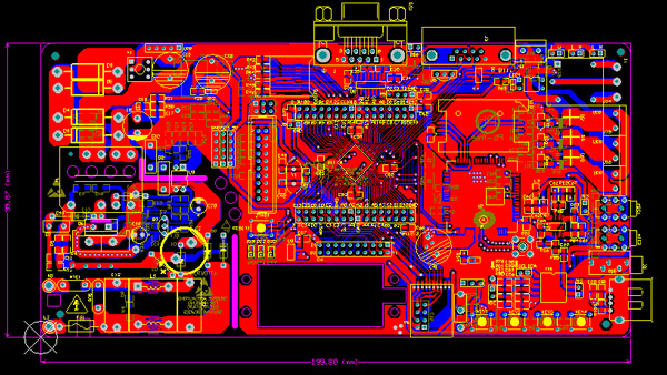
(1) When designing the pad of through hole components, the size of the pad shall be appropriate. If the solder pad is too big, the solder spreading area is large,then the solder joint is not full;if the solder pad is too small,the surface tension of copper foil will be small, then the solder joint will become non-wetting solder joint. The gap between the aperture and the component pin is too large, which is easy to cause dry joint. When the aperture is 0.05 - 0.2mm wider than the component pin and the pad diameter is 2 - 2.5 times of the aperture, it is an ideal condition for soldering.
(2) When designing the pad of SMD components, the following points should be considered: in order to eliminate the "shadow effect" as much as possible, the welding end or pin of SMD should be facing the direction of tin flow, so as to facilitate the contact with tin flow and reduce dry joint and missing soldering. The smaller components should not be arranged after the larger components, so as to prevent the larger components from hindering the tin flow from contacting the pad of the smaller components and causing solder leakage.

2. Flatness control of PCB
Wave soldering has high requirements on the flatness of the printed circuit board. Generally, the warpage shall be less than 0.5mm. If it is greater than 0.5mm, it shall be leveled. In particular, the thickness of some circuit boards is only about 1.5mm, which has higher requirement on warpage. Otherwise, the soldering quality cannot be guaranteed. The following matters should be paid attention to:
(1) The PCB boards and components store properly and shorten the storage cycle as far as possible. During PCB welding process, copper foil and component leads without dust, grease and oxide are conducive to the formation of qualified solder joints. Therefore, the printed circuit boards and components should be stored in a dry and clean environment and shorten the storage cycle as far as possible.
(3) For PCB boards which stored for a long time, the surface of the PCBs should be cleaned to improve solderability, and reduce dry solder and solder bridge. For component pins with a certain degree of oxidation on the surface, the surface oxide layer should be removed first.

2、 Quality control of process materials
In wave soldering, the main process materials are flux and tin soldering.
1. The use of flux
The flux can remove the oxide on the welding surface, prevent the solder and welding surface oxidation again during welding,and reduce the surface tension of solder, to help transfer heat to the welding area. Flux plays an important role in the control of welding quality.
2. Quality control of solder
Tin lead solder is continuously oxidized at high temperature (250 ℃), which makes the content of tin from the solder in the tin pot continuously decrease and deviate from the eutectic point, resulting in poor fluidity, it will cause dry joint, solder bridge,insufficient solder joint and other quality problems.

3、 Parameter control in soldering process
The influence of technology parameters on the PCB assembly quality is complex, mainly including the following points:
1. Control of preheating temperature
Function of preheating: Make the solvent in the flux fully volatilize, so as not to affect the wetting of the printed circuit board and the formation of solder joints when the printed board passes through the solder; Make the circuit board reach a certain temperature before welding to avoid warping deformation caused by thermal shock. According to our experience, the preheating temperature is generally controlled at 180 ℃ to 200 ℃, and the preheating time is 1 - 3 minutes.
2. Soldering orbital inclination
The influence of orbital inclination is very important on pcb soldering, especially for high-density SMT components. When the inclination angle is too small, it is easy to cause solder bridge, especially the "shielding area" of SMT components is more likely to cause solder bridge; When the inclination angle is too big,although it's conducive to the elimination of bridging, but the tin consumption of solder joints is too small, which is easy to cause dry joint. The track inclination shall be controlled between 5 ° - 7 °.

3. Wave crest height
The height of wave crest will change due to the PCBA welding time. Appropriate correction shall be made in the welding process to ensure the ideal height. The height of wave crest for welding shall be subject to the tin pressing depth of 1 / 2 - 1 / 3 of the thickness of PCB board.
4. Welding temperature
Welding temperature is an important process parameter affecting welding quality. When the welding temperature is too low, the expansion rate and wetting ability of solder become poor, so that the solder pad or the solder pin of components can not be fully wetted, resulting in defects such as dry joint, sharpening, bridging and so on; When the welding temperature is too high, it will speed the oxidation of pad, component pin and solder, which is easy to cause dry joint
Hot Products
Navigation
+86 134 0021 8776
Floor 9, Aupu building, No. 395 XinShi North Road, Shijiazhuang Hebei, China
Request a Quote
