+86 134 0021 8776
+86 134 0021 8776
News
Jan. 09, 2024
As the package density of integrated circuits increases, and leads to high concentration of interconnects, this makes the use of multiple substrates necessary.


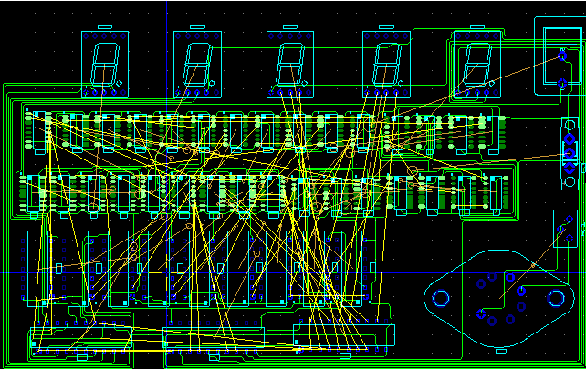
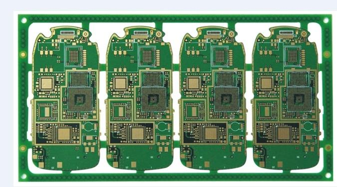
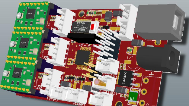
Requirements for the design of multilayer PCB circuit boards:
1.Requirements for wires, cloth layers, wiring area.
Multilayer printed wiring is performed by circuit function, In outer wiring, wiring is required on the weld surface, component less wiring, It is beneficial to the maintenance and troubleshooting of the printed circuit board. A large area of copper foil should be evenly distributed inside and outside, This will help to reduce the warpage of the board, and also to obtain a more uniform coating on the surface during electroplating.

2.Determination of shape, size and number of plates
The printed circuit board has the problem of assembling with other structure parts, therefore, the shape and size of the PCB board must be based on the overall structure of the product. But from the point of view of production technology, should be as simple as possible, In order to facilitate assembly, improve production efficiency, reduce labor costs.

3.Location and orientation of components
Position and direction of components, First of all, the circuit principle should be considered, cater to the direction of the circuit. Whether the placement is reasonable or not will directly affect the performance of the printed circuit board. Reasonable placement of components, in some sense, has heralded the success of the printed circuit board design. So, when beginning to compile PCB layout, decided to set the overall layout, the circuit principle should be analyzed in detail.

4.Requirements for traverse and linewidth
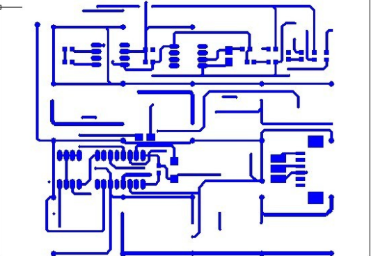
The line of the multilayer plate should separate the power layer, formation and signal layer, reduce interference between power, ground, and signal. The lines of the adjacent two layers of printed boards should be perpendicular to each other or diagonal lines or curves, so that parallel lines can not be used to reduce interlayer coupling and interference. And the conductor should try to use the short line, especially for small signal circuit, the shorter the line, the smaller the resistance, the smaller the interference.

5.Requirements for safe spacing
The setting of safety intervals shall meet the requirements of electrical safety. In the case of wiring can be arranged, the spacing should be taken as large as possible, in order to improve the rate of finished products and reduce the failure of the finished product board.
Previous: How to choose the substrate of FPC board
Next: FPC welding procedure
Hot Products
Navigation
+86 134 0021 8776
Floor 9, Aupu building, No. 395 XinShi North Road, Shijiazhuang Hebei, China
Request a Quote
