+86 134 0021 8776
+86 134 0021 8776
Jul. 24, 2023
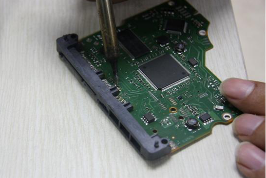
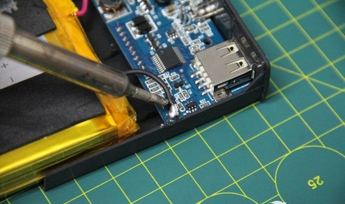
* After all the pins have been welded, soak all pins with solder to clean the solder. Suck out excess solder tin where needed, to eliminate any short circuit and lap joint. Finally, check whether there weld with tweezers. When the inspection is complete, remove the solder from the circuit board, until the solder is gone.

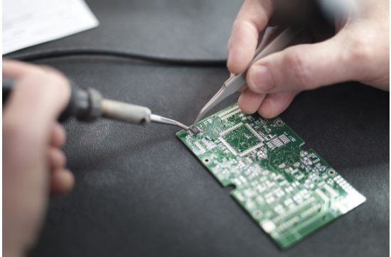
* The circuit board welding engineer reminds you that the patch resistance component is relatively easy to solder, Tin can be first placed on a solder joint, and then put one end of the component, clamp the element with tweezers, and let's see if we've got it right. It takes a lot of practice to really master welding skills.

* Apply the soldering flux to the pad before welding, Iron it again, In case the tin plate is badly damaged or oxidized.

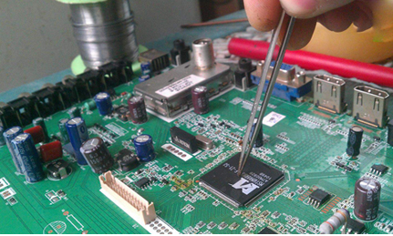
* Put the PQFP chip on the PCB board with tweezers carefully, be careful not to damage the pins. Align it with the pads and make sure the chips are in the right direction. Turn the temperature of the soldering iron to more than 300 degrees centigrade, attach a small amount of solder to the tip of the iron, Chip down the aligned position by means of a tool, Add a small amount of solder to the pins on the two diagonal positions, still press down chip, Fix the chip and not move it. If necessary, adjust or remove and re position on the PCB board.

* When soldering all the pins, solder the tip of the soldering iron, apply all the pins to the solder so that the pins remain moist. Contact the end of each pin of the chip with the tip of the soldering iron until the solder flow pin is seen. When soldering, keep the iron tip parallel to the soldered pin to prevent overlap due to excessive soldering.

Previous: The names of the layers of the Gerber file and the layers of the original PCB
Next: PCB laminated design multi-layer board need to pay attention to matters
Hot Products
Navigation
+86 134 0021 8776
Floor 9, Aupu building, No. 395 XinShi North Road, Shijiazhuang Hebei, China
Request a Quote
