+86 134 0021 8776
+86 134 0021 8776
Oct. 26, 2022
1.PCB board material
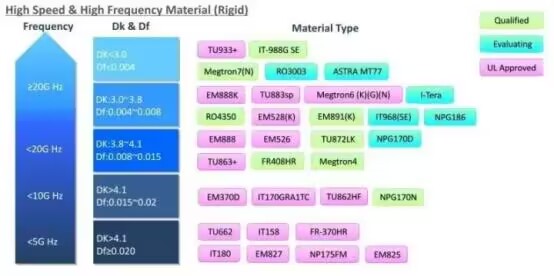
The commonly used plates are as follows. The most familiar is FR-4, which uses fiberglass cloth as the reinforcement material and epoxy resin as the binder.
It is also divided into low/middle/high Tg, is the maximum glass transition temperature can withstand.
It is the maximum rated working temperature of the plate. Generally, a little more High-Tg is chosen (about TG170).
Our commonly used FR-4 has the highest material loss ranking, but FR-4 is collectively referred to, such as TU662, IT158.

The plate is mainly classified according to Dk/Df, Dk is the relative dielectric constant, Df is the loss factor.
The greater the relative permittivity, the slower the signal propagates in the medium.
Therefore, in the design of high-speed signal PCB, the material with small dielectric constant and material loss factor will be selected as far as possible, and accordingly, the cost will be higher.
Layout Engineers first evaluate the number of layers required by the PCB and determine the layup design and line width and line spacing. Line width and line spacing are used to control the characteristic impedance of signal cables
PCB thickness is not arbitrary. Common ones such as 1mm, 1.6mm, 2mm, 2.4mm
Because PP, CORE thickness can not be infinite or infinitesimally small, there is a certain thickness range.
Therefore, for a certain PCB board thickness, such as 1.6mm, the maximum number of laminated layers is limited.
Generally 1.6mm board thickness, PCB can be stacked up to about 14 layers.
2.Recommended method for stacking six layers PCB

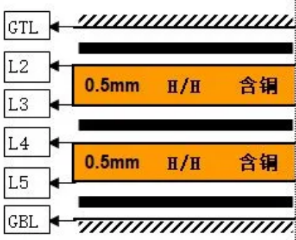
Stack up with two core panels + two copper foils
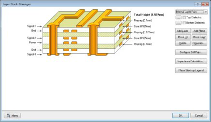
2.1.SIG-GND-SIG-PWR-GND-SIG;


Stack-up of 6-layers PCB

For this scheme, the laminated scheme can
obtain better signal integrity. The signal layer is adjacent to the grounding layer, and the power layer is paired with the grounding layer. The impedance of each routing layer can be controlled well, and both strata are magnetic force lines that can absorb well. And in the case of complete power supply, the formation can provide a better return path for each signal layer.
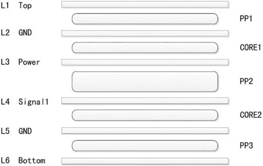
2.2 GND-SIG-GND-PWR-SIG -GND;
For this scheme, this scheme is only applicable to the case when the device density is not very high. This layer has all the advantages of the upper layer, and the ground plane of the top and bottom layer is relatively complete, which can be used as a better shielding layer. It is important to note that the power supply layer should be close to the layer that is not the main component surface, because the underlying plane will be more complete. Therefore, EMI performance is better than the first scheme.
Previous: SMT processing process
Next: What is the difficulty in the production process of multilayer PCB circuit board?
Hot Products
Navigation
+86 134 0021 8776
Floor 9, Aupu building, No. 395 XinShi North Road, Shijiazhuang Hebei, China
Request a Quote
