+86 134 0021 8776
+86 134 0021 8776
Nov. 30, 2023
PCB board component patch welding has two welding methods, respectively, wave soldering and reflow welding,let’s introduce these two welding methods as followings.
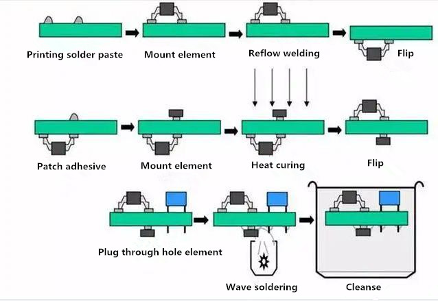
We know that wave soldering is usually used to weld plug-in devices, reflow welding is usually used to weld patch devices, and the current PCB board is relatively complex, basically including patch devices and plug-in devices. Therefore, when the patch welding is done in the patch factory, the patch device is first welded by reflow welding, and then the plug-in device is welded by wave soldering.
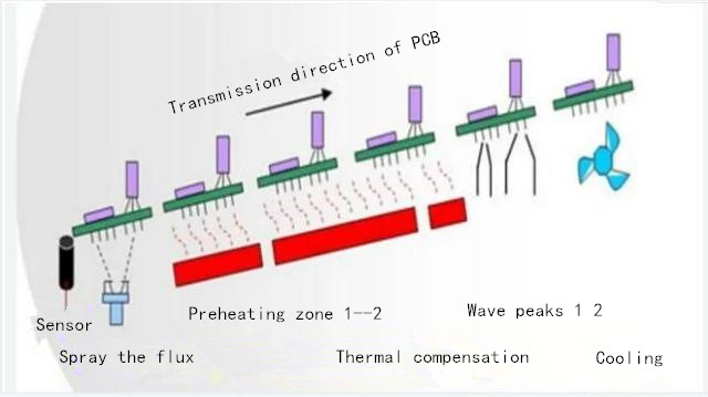
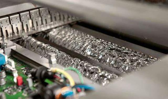
1.Wave soldering is usually the direct contact of the welding surface with the solder after melting at high temperature to form a wave peak to achieve the purpose of welding, usually the use of electric pump to melt the solder spout to form a wave peak for welding, so in the process of wave soldering, the welding surface of our circuit board will not contact the solder at the same time, the circuit board is generally placed on the conveyor belt. According to a certain speed through the solder peak, usually the solder on the welding surface will not stay for a long time.
The working process of wave soldering is generally to first plug in and then apply our flux in the form of spray, and then preheat, preheating can reduce the thermal shock generated when the component enters the wave peak, and after preheating, wave soldering is carried out. When the circuit board enters the wave peak, the direction of the solder flow and the direction of the board forward are opposite, and all the flux around the component can be removed. At this time, after the solder joint reaches the temperature, the device can be welded firmly, and then it can be cooled.
2.Reflow welding refers to heating and melting the solder paste (the solder paste is generally composed of a mixture of tin powder and flux), so that it can return to the flowing liquid state (this process is reflux), so that the device pre-placed on the solder pad and the solder are fully in contact with the solder to achieve the purpose of welding.
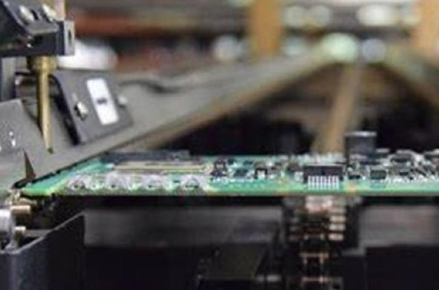
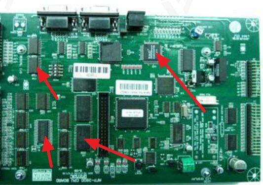
The workflow of reflow welding is generally to first open the steel mesh according to our PCB, so that the mesh on the steel mesh corresponds to the solder pad of the board, so that in the next process of brushing the solder paste, each solder pad can have enough solder paste, and then the components can be placed in the solder pad, generally our placing order is from left to right, from top to bottom, from large to small. At the same time, it is also necessary to pay attention to the direction of the device identification, after being placed, you can enter the reflow welding production line above processing, in the machine will first go through the preheating zone, constant temperature zone, welding zone, cooling zone, etc., after the previous step of processing after the board check that there is no problem, you can carry out the next production process, the essence of reflow welding is to control the temperature to complete the welding.

The above is the process of reflow soldering, then usually our PCB board has devices at the top and bottom, then the above process will be passed through again at this time, and now the first side is pre-coated with tinning paste. After welding and cooling, the second side is pre-coated with solder paste, and then the patch is applied, and then the welding is cooled. Therefore, when there are devices on both sides, we should pay attention to placing the heavy devices on one side as far as possible, which can also ensure the reliability of welding.
Previous: FPC welding procedure
Hot Products
Navigation
+86 134 0021 8776
Floor 9, Aupu building, No. 395 XinShi North Road, Shijiazhuang Hebei, China
Request a Quote
